
Precision lapping, done right.
Chicago Lapping Co handles contract lapping for shops that need flat, parallel, and smooth surfaces — single- and double-sided, production lots, seals, wafers, and specialty work. Send a drawing. Get a straight answer.
Lapping services
These processes are available across Illinois, Wisconsin, and Indiana. Work is performed under documented process controls aligned with ISO 9001:2015. One request gets you process guidance, realistic tolerances, and lead time — usually within a business day.
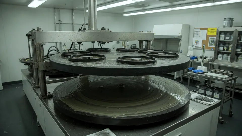
Single and Double-Sided Lapping
Both faces finished in one setup. Parallelism and flatness held together for seals, plates, and high-volume blanks.
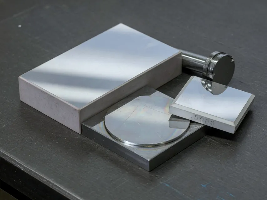
Flat lapping
Planar finishing for reference faces, tooling, and inspection surfaces where flatness drives the whole measurement chain.
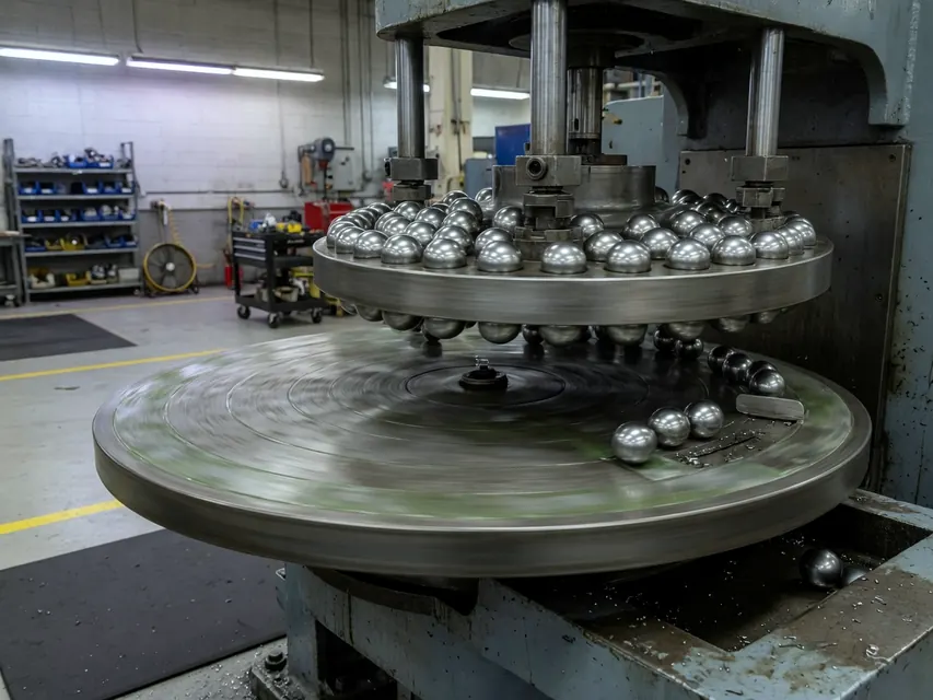
Spherical/Ball Lapping
Controlled spherical and ball geometry finishing for valves, bearings, and precision mating surfaces.
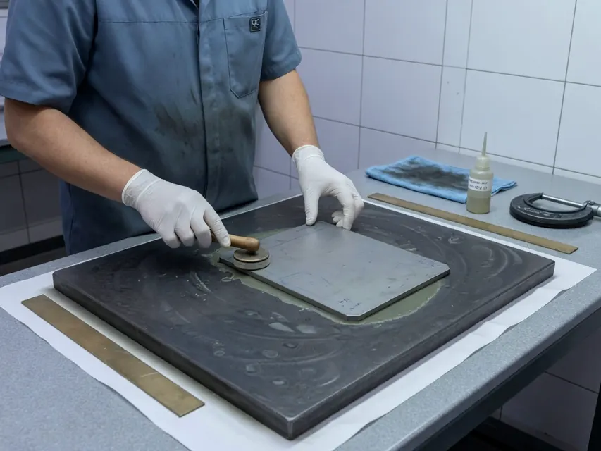
Hand lapping
Manual finishing for prototypes, selective fits, and geometry that machine cycles cannot reach cleanly.
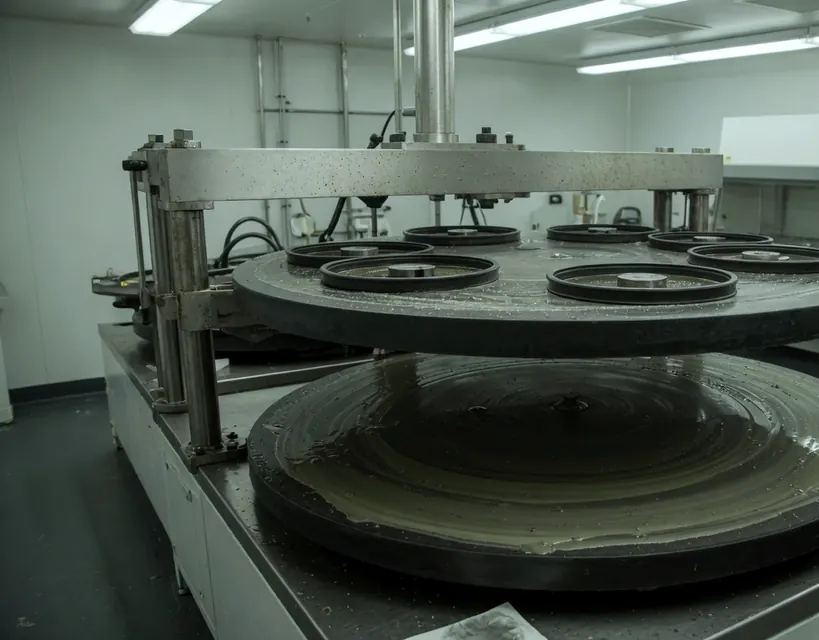
Machine lapping
Repeatable machine cycles for production lots with documented flatness and surface-finish targets.
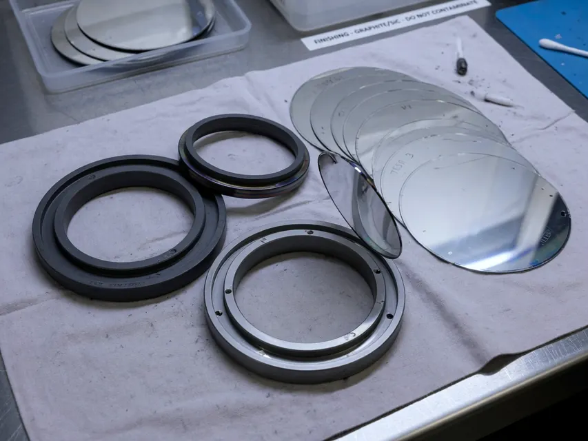
Mechanical Seal/Silicon Wafer Lapping
Seal faces and wafer blanks finished for contact integrity, low Ra, and lot-consistent geometry.
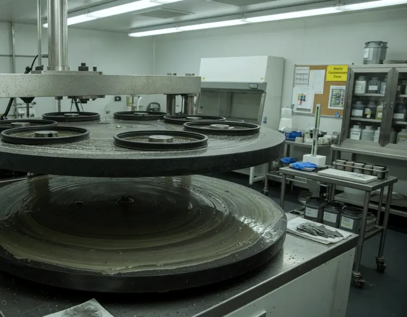
Production lapping
Scheduled lot work with process controls, inspection sampling, and per-lot certification packages.
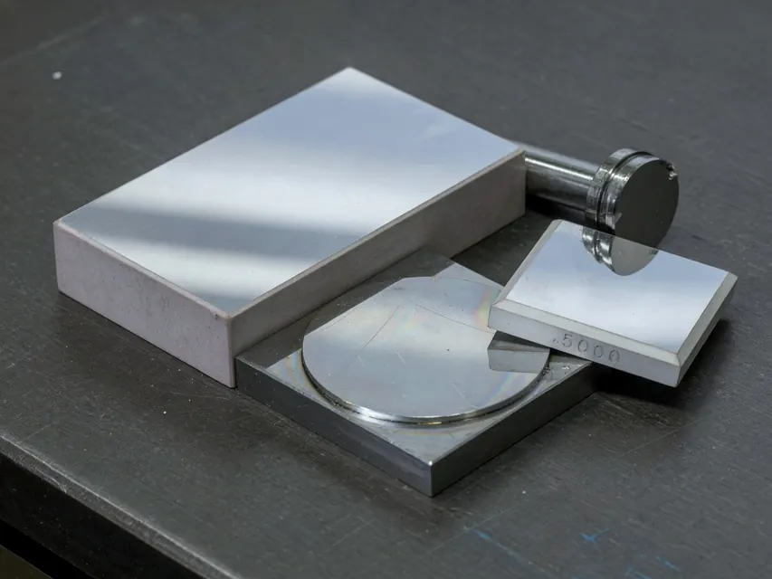
Taper, Shoulder, and Counter Bore Lapping
Targeted finishing on shoulders, tapers, and counterbores where form error shows up as assembly failure.
Simple from start to finish
No portals. No runaround. A straightforward path for shops that need parts lapped to print.
Send a quote request
Drawings, material, target flatness or finish, and quantity. Email and phone work too.
Get a clear plan
Process, achievable tolerances, and timing are confirmed before parts move.
Parts are lapped
Work is performed under documented process controls aligned with ISO 9001:2015.
Inspected and shipped
Flatness and finish are checked. Lots go out with inspection records.
Measured, not guessed
Flatness is checked — not assumed. Lots are verified with laser interferometry, white-light profilometry, stylus roughness, and air gaging on temperature-stable benches. Results are tied to calibrated standards.
- Laser InterferometryFlatness / Form
- White-Light Profilometry3D Surface Texture
- Stylus ProfilometerRa / Rz Roughness
- Air GagingThickness / Parallelism
The numbers that matter
Coverage, process range, and inspection — plain facts for buyers comparing shops.
What can be held by material
| Material Class | Typical Applications | Min Thickness | Flatness | Ra |
|---|---|---|---|---|
| Technical Ceramics (Al₂O₃, AlN) | Semiconductor chucks, seals | 0.005" | 1 light band | < 1 µin |
| Silicon Carbide (SiC) | Optics, wafer handling | 0.010" | 1/4 light band | < 0.5 µin |
| Tool Steels / Tungsten Carbide | Stamping dies, cutting tools | 0.002" | 2 light bands | < 2 µin |
| Exotic Alloys (Ti, Inconel) | Aerospace components, medical | 0.015" | 2 light bands | < 4 µin |
| Optical Materials (Sapphire, Fused Silica) | Windows, lenses, substrates | 0.004" | 1/10 light band | Sub-angstrom |
| Silicon Wafers | CMP, bonding, MEMS substrates | 0.005" | 1/4 light band | < 0.5 µin |
Illinois, Wisconsin, and Indiana
Precision lapping coverage spans Illinois , Wisconsin , and Indiana , with dedicated landing pages for every metropolitan area in the index below.
View metropolitan coverage list
Local-pickup and freight coverage includes Chicago , Aurora , Schaumburg , Elgin , Joliet , Rockford , Milwaukee , Madison , Green Bay , Kenosha , Racine , Appleton , Waukesha , Indianapolis , Fort Wayne , Evansville , South Bend , and Hammond . Each city page covers the lapping processes available in that metro, typical lead times, and how to submit for a direct quote.
Illinois, Wisconsin & Indiana — 18 metro areas
Cities Browse by area
Tell us about the part
Most quotes come back within one business day. Include drawings if you have them, the finish you need, and how many pieces. You'll get achievable flatness, timing, and pricing for the job.
- Phone(618) 323-0428
- Email[email protected]
- HoursMon–Fri, 7am–5pm CT
- TurnaroundAbout 1 business day